Peking University, September 20, 2022: Scaling down the size of field-effect transistors (FETs) in integrated circuits leads to higher switching frequency and integration density, but also results in degraded switch-off behavior due to the short-channel effects. To mitigate these effects, transistors made of high-mobility two-dimensional (2D) semiconductor channels and ultrathin dielectrics with sub-0.5-nm-EOT (equivalent oxide thickness) are required by the International Roadmap for Devices and Systems (IRDS). However, the integration of both is still challenging. Recently, Peng Hailin’s research group has reported the synthesis of a single-crystalline native oxide dielectric, β-Bi
2SeO
5,
via an ultraviolet-assisted intercalative oxidation of high-mobility 2D semiconductor Bi
2O2S
e. Single-crystalline β-Bi
2SeO
5 has excellent insulativity and high dielectric constant of around 22, and can be scaled down to an EOT of 0.41 nm in 2D FETs, with leakage current below the low-power limit, meeting the requirements of IRDS. This research entitled “
A single-crystalline native dielectric for two-dimensional semiconductors with an equivalent oxide thickness below 0.5 nm” has been published by
Nature Electronics on Sept. 15th, 2022.
Scaling down the size of field-effect transistors (FETs) in integrated circuits leads to higher switching frequency and more devices integrated on a single chip. However, when the length of the semiconductor channel is less than 6 times the characteristic length, the switch-off behavior is degraded due to the short-channel effect, leading to a reduced frequency and higher power consumption. The characteristic length lambda is defined as: √((ε
bt
bt
ox)⁄(nε
ox )), where n is the effective gate number, and t
b (ε
b) and t
ox (ε
ox) are the thicknesses (dielectric constants) of the semiconductor body and oxide dielectric, respectively. Thus, using transistors made of two-dimensional (2D) semiconductor channels and ultrathin dielectrics with high dielectric constant can minimize lambda and mitigate the short-channel effects.
However, it remains a challenge to integrate 2D semiconductors with dielectrics that have sub-0.5-nm EOT (equivalent oxide thickness) and low leakage current, as required by IRDS. Dielectrics on 2D semiconductors, including HfO
2, hBN and CaF
2, cannot be scaled down to an EOT of less than 0.9 nm, owing to issues such as poor insulativity or low dielectric constant. Thus, a new ultrathin dielectric with high dielectric constant and excellent insulativity is urgently required for 2D electronics.
Prof. Peng Hailin’s group developed a high-mobility 2D semiconductor Bi
2O2S
e (
Nature Nanotechnology 2017, 12, 530), and have been working on the oxidation of Bi
2O
2Se. Bi
2O
2Se has been transformed into polycrystalline or amorphous native oxide dielectric Bi
2SeO
5 via thermal oxidation (
Nature Electronics 2020, 3, 473) or oxygen plasma treatment (
Nano Letters 2020, 20, 7469). High-performance 2D Bi
2O
2Se FETs and inverter circuits were fabricated (
Acc. Mater. Res. 2021, 2, 842-853), in which the native oxide dielectrics can be scaled down to an EOT of 0.9 nm.
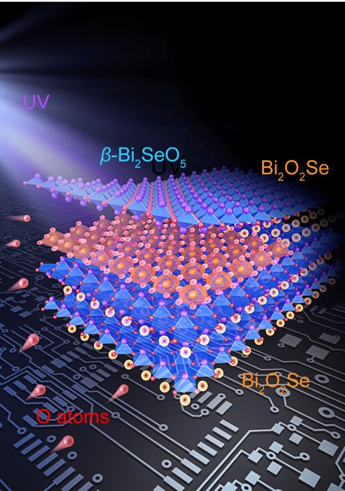
Fig. 1 Diagram of the UV-assisted intercalative oxidation of 2D Bi
2O
2Se for single-crystalline native oxide dielectric β-Bi
2SeO
5.
Recently, inspired by the zipper-like layered structure of 2D Bi
2O
2Se and the intercalation of 2D materials, Peng’s research group developed a UV-assisted intercalative oxidation process of 2D Bi
2O
2Se (Fig. 1). The Bi-O framework of the precursor remains intact throughout the process (Fig. 2a), and thus the native oxide dielectric, a new phase of Bi
2SeO
5 (named β-Bi
2SeO
5), inherits the single-crystalline characteristic of the Bi
2O
2Se precursor. The UV-assisted intercalative oxidation is compatible with UV lithography, and with a special lithography mask, wafer-scale area-selective oxidation can be achieved (Fig. 2b). 2D Bi
2O
2Se can also be oxidized layer-by-layer, and an atomically-flat lattice-matched interface can be obtained.
The single-crystalline β-Bi
2SeO
5 can serve as a high-performance dielectric in Bi2O2Se-based 2D FETs, owing to the atomically-flat lattice-matched interface, thickness-independent high dielectric constant of around 22, and excellent insulativity. 2D transistors fabricated with β-Bi
2SeO
5/Bi
2O
2Se heterostructure show high electrical performance, including a mobility of 427 cm
2·V
–1·s
–1, hysteresis as low as 20–60 mV, and subthreshold swing (SS) below 65 mV·dec
–1. In addition, even the thinnest β-Bi
2SeO
5 dielectric we used in 2D FETs, at an EOT of only 0.41 nm, still has a gate leakage current below the low-power limit of 0.015 A·cm
–2 at 1 V gate voltage, meeting the requirements of IRDS.
The EOT or ECT (effective capacitance thickness) and leakage current density of common dielectrics have been reviewed for comparison. As shown in Fig. 2c, the single-crystalline β-Bi2SeO5 outperforms other dielectrics such as ALD-synthesized HfO2, hBN, single-crystalline CaF2 and polycrystalline α-Bi2SeO5. With a leakage current below the low-power limit (0.015 A·cm
−2 at 1 V), single-crystalline β-Bi
2SeO
5 meets the requirement of EOT < 0.5 nm and ECT ≤ 0.9 nm in IRDS. The single-crystalline dielectric β-Bi
2SeO
5 fills the gap of sub-0.5-nm-EOT dielectric in 2D transistors, and thus holds great promise for the future of 2D electronics.
Fig. 2 Synthesis and properties of the single-crystalline native oxide dielectric β-Bi
2SeO
5. a, Microscopic process of the intercalative oxidation. b, Wafer-scale area-selective oxidation for Bi
2O
2Se/β-Bi
2SeO
5 heterostructure. c, Comparison of single-crystalline β-Bi
2SeO
5 and common dielectrics in terms of EOT or ECT versus leakage current density at 1 V gate voltage.
This article was published online by
Nature Electronics on Sept. 15th, 2022. The corresponding author of this article is Prof. Peng Hailin, and the first author is Zhang Yichi, both from College of Chemistry and Molecular Engineering, Peking University. Other collaborators include Prof. Lai Keji at the University of Texas at Austin and Prof. Gao Peng at Peking University. For a brief introduction to this work, a Research Briefing entitled “Producing ultrathin monocrystalline native oxide dielectrics for 2D transistors”, finished by Prof. Peng Hailin and Zhang Yichi on behalf of all the authors, was published in Nature Electronics at the same time.
This work was supported by the National Natural Science Foundation of China, Beijing National Laboratory for Molecular Sciences, Tencent Foundation, and Molecular Materials and Nanofabrication Laboratory (MMNL) in the College of Chemistry and Molecular Engineering of Peking University.
Link to the article:
https://www.nature.com/articles/s41928-022-00824-9
Edited by: Meng Bin
Source: College of Chemistry and Molecular Engineering