Peking University, Aug. 27, 2018: Sensing infrared (IR) light beyond silicon’s detection limit (l > 1.1 mm) has been deeply embedded in modern technology and human society with diverse applications. Among the infrared wavelength range of 0.7mm to 1 mm, the spectral region between 1 mm and 1.8 mm has attracted particular commercial interest due to low silica and water absorption in this range, with applications such as high speed fiber-optic telecommunications (~1.55 mm) and anatomic-feature detection. As for detecting infrared light, the progress has always been driven by the discovery of new photodetection materials, from the II-VI compounds of HgxCd1-xTe to III-V ones of InxGa1-xAs in bulk form. During the past 20 years, as the market grows, it is becoming increasingly important to find materials which are compatible with well-developed silicon readout circuit such as complementary metal-oxide semiconductor (CMOS). The detectors based on these materials can thus be fabricated with silicon industry techniques, reaching lower cost, larger number of pixels on focal plan arrays (FPA), higher frame rates and more on-chip signal-processing functions.
On the other hand, the recent rise of two-dimensional (2D) layered materials, with strong light-matter interactions and dangling-bond-free surfaces, has brought up new possibilities for high-performance photodetection, which may adapt to silicon readout circuits. An ideal IR detector of 2D materials should respond fast and sensitively. However, the existing 2D layered materials either have too large band gaps to detect IR light, such as transition metal dichalcogenides, or exhibit sensitivity lower than tens of mA/W such as graphene. Therefore, identifying new 2D layered materials for sensitive and high-speed IR detection is strongly motivated and could potentially lead to revolutionary applications of IR detection.
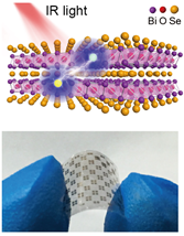
During the past two years, Professor Peng Hailin’s group in College of Chemistry and Molecular Engineering, Peking University, together with their collaborators, have found a new 2D material—Bi2O2Se with ultrahigh carrier mobility (~28900 cm2/Vs at 1.9 K and ~450 cm2/Vs at room temperature), suitable electronic band gap (~0.8 eV) and stability in ambient air. This new 2D material has shown extraordinary properties in field-effect transistor and quantum transport [Nature Nanotech. 2017, 12, 530; Nano Lett. 2017, 17, 3021; Adv. Mater. 2017, 29, 1704060].
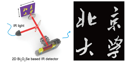
Recently, they have demonstrated that photodetectors based on Bi2O2Se crystals on flexible substrates have a high sensitivity (~65 A/W at 1200 nm) and wide detecting spectrum from visible to 1.7 mm. By adopting time-resolved photocurrent spectroscopy, they have found that the Bi2O2Se detectors have ultrafast intrinsic photoresponse of ~1 ps at room temperature, indicating the detectable frequency limit up to ~500 GHz. Furthermore, they have shown that Bi2O2Se photodetectors have imaging capability by two approaches. One is by scanning single-pixel photodetector along the optical imaging plane, while the other is to show the detecting pattern by using a 35 multi-pixel arrays. As 2D Bi2O2Se is potentially compatible with silicon readout circuit, and has mass production capability, it may open new possibilities in low-cost, highly-sensitive, high-speed, and flexible infrared photodetection and imaging at room temperature.
The corresponding paper has been published in Nature Communications 9, 3311 (2018) with the title of Ultrafast and highly sensitive infrared photodetectors based on two-dimentional oxyselenide crystals. The equally-contributed first authors are Yin Jianbo, Tan Zhenjun, Hong Hao and Wu Jinxiong. The corresponding authors are Peng Hailin and Liu Kaihui. This work have been sponsored by Ministry of Science and Technology of China, and National Natural Science Foundation of China.
Edited by: Zhang Jiang
Source: College of Chemistry and Molecular Engineering